Products & capabilities

Substrates, deposition materials and processed research samples.

A focused portfolio for semiconductor and advanced-materials laboratories, from a single research wafer to application-led processed sapphire substrates.

01SUBSTRATES

Wafers & Research Substrates

Single-crystal substrates for epitaxy, device fabrication, MEMS, optical coatings and process development.

  • Silicon: CZ & FZ, prime and monitor grade
  • Sapphire: C-, A-, R- and M-plane
  • Silicon carbide: 4H-SiC and 6H-SiC
  • Custom orientation, thickness, polish and size
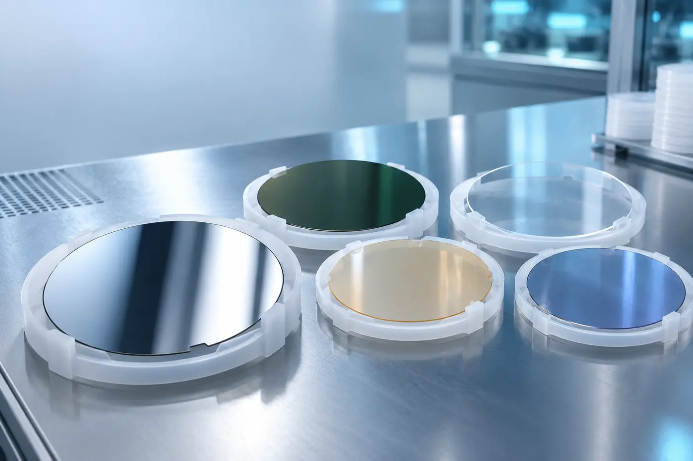
Silicon and sapphire wafers in protective carriers on a laboratory surface
Representative wafer formats
02TARGETS

Sputtering Targets

High-purity PVD materials in standard and custom geometries, with target bonding options.

  • Pure metals and metallic alloys
  • Oxides, nitrides and compound materials
  • 2-inch and custom-size targets
  • Backing plates and bonding services
03EVAPORATION

E-Beam & Thermal Materials

Deposition materials selected for purity, form, source compatibility and the intended thin-film application.

  • Pellets, granules, wire, slugs and pieces
  • Metals, alloys, oxides and fluorides
  • E-beam crucible liners
  • Thermal boats, filaments and baskets
04PROCESSED

Processed Substrates

Research-scale sapphire substrates processed through selected CVD and PVD routes, with emphasis on wide-bandgap oxide development.

  • Present focus: gallium oxide films on sapphire
  • Current routes: LPCVD and mist CVD, with PVD support as required
  • Current formats: 1 x 1 cm, 1 inch and 2 inch
  • Development roadmap: 4 inch formats and MOCVD capability
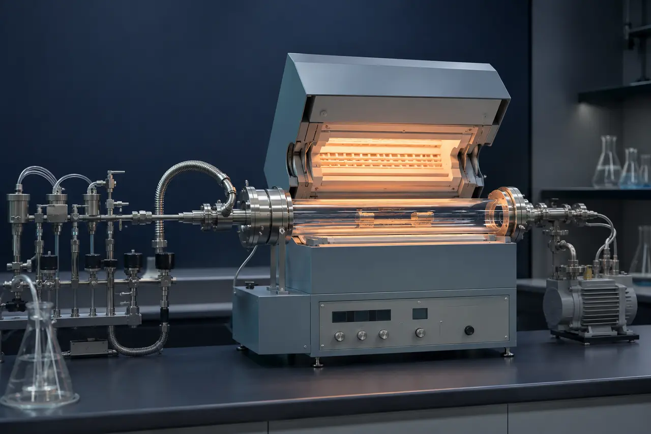
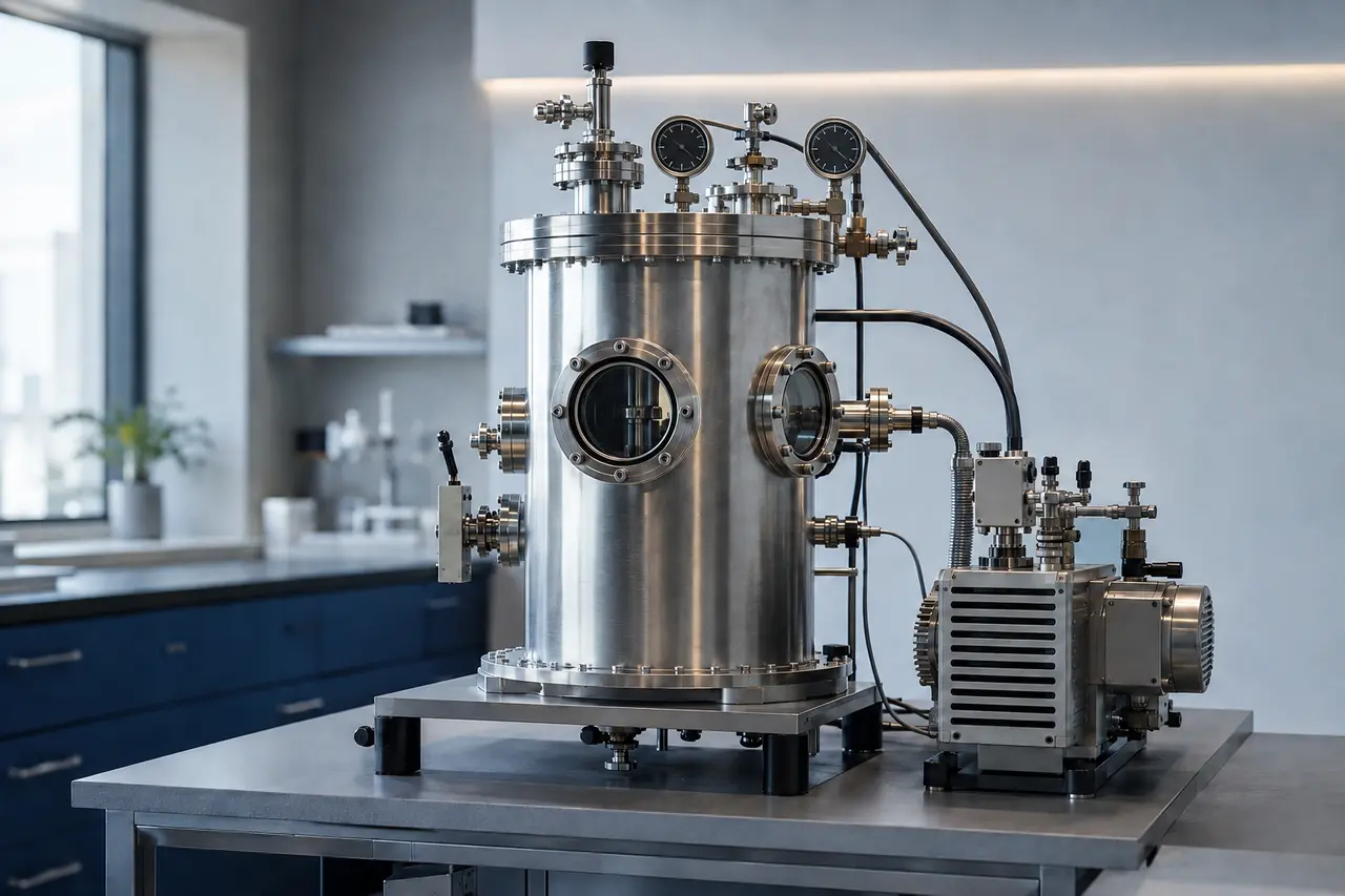
Research-scale deposition equipment used for processed substrate development
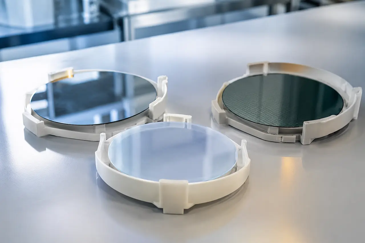
Representative processed-substrate development environment

Representative images are provided for application guidance. Final materials, dimensions and system configurations depend on project requirements.

Specification guidance

Details that help us quote accurately.

These fields are a practical starting point. Final specifications are confirmed against the application and the selected supply route.

Wafers and research substrates

ParameterExamples to provideWhy it matters
MaterialSilicon, sapphire, SiC or another substrateDefines the crystal and process family
Diameter and thicknessNominal size, tolerance and quantityConfirms tool and holder compatibility
OrientationCrystal plane, off-cut and direction if applicableAffects growth and device processing
Surface and gradeSingle-side or double-side polish, prime, monitor or research gradeSets surface quality and inspection level
Electrical propertiesDopant, conductivity type and resistivity rangeConfirms electrical behaviour

Targets and evaporation materials

ParameterExamples to provideWhy it matters
CompositionElement, alloy, oxide, nitride or compoundIdentifies the required material route
PurityRequired grade or minimum percentageControls impurities in the deposited film
Form and dimensionsTarget diameter and thickness, pellets, granules, wire or piecesMatches the deposition source
Backing and bondingBacking plate material and preferred bonding methodSupports thermal and mechanical compatibility
QuantityNumber of targets or net material weightSupports price and delivery planning

Processed sapphire substrates

ParameterExamples to provideWhy it matters
Film or materialGallium oxide or another oxide compositionDefines the material and process route
Deposition routeLPCVD, mist CVD or a selected PVD methodSets the process architecture and precursor needs
Sapphire format1 x 1 cm, 1 inch or 2 inch, with orientation if requiredConfirms substrate and holder compatibility
Film targetThickness, uniformity, coverage and surface requirementsDefines the acceptance criteria
Phase and dopantBeta-phase gallium oxide or a doped composition such as SnGuides material and process development
CharacterisationRequested structural, optical, surface or electrical measurementsConfirms what evidence is required with the sample

Indicative specifications for inquiry planning. Final configuration is confirmed against application requirements.

Custom specifications welcome

Tell us the material, grade, purity, geometry or process window.

Request a quotation